Head of the Group

Grzegorz Sęk
office: 356A, A-1
phone: +48 71 320 45 73
Research
The research concentrates on application of complementary techniques of optical spectroscopy for investigations of epitaxial nanostructures, mostly quantum dots (QD), dedicated for optoelectronic devices operating in the near infrared spectral range, with a strong focus on telecom windows. The studies concern both ensembles of quantum dots, with application prospects as active material for telecom lasers or optical amplifiers, and single quantum emitters, investigated as potential sources of single photons and entangled photons for quantum communication, taking advantage of existing fibre-optical infrastructure.
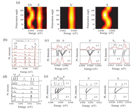
Photoreflectance (PR) spectroscopy, a variant of a modulation absorption-like technique, is used for determination of the hierarchy of confined states, photoluminescence (PL) gives insight into the optical quality of structures and their emission properties, photoluminescence excitation (PLE) spectroscopy allows investigating carrier transfer processes. Beside experiments on ensembles of dots, the group carries out also PL and PLE measurements on single emitters, also in an external magnetic field. After initial analysis of a power- and polarization-dependence of emission lines from nanoobjects, suitable candidates undergo more sophisticated investigations by means of correlation spectroscopy in Hanbury-Brown and Twiss mode in order to determine emission statistics, in particular to study non-classical character of emission. In the case of multiphoton cascades, potential quantum entanglement is evaluated. Experimental results are supported by 8‑band k∙p calculations for realistic geometries of emitters.
Activities
Ensembles of QDs for laser applications
Tunnel injection structures
Many theoretical papers, as well as numerous experimental works, have shown the advantages of QD-based lasers in a multitude of applications in comparison to quantum well (QW) based devices. They were characterised by ultralow threshold currents, better temperature stability, and a broad gain spectrum, enabling large range of wavelength tuning. However, despite many demonstrations of their advantages, they fail to satisfy the expectations, especially in the crucial telecom windows, at 1.3 and 1.55 µm.
Two major limitations that stand in a way of success stem from the three-dimensional confinement potential of QDs and low total density of states related to it. It results in low efficiency of carrier collection by the dots, adversely affecting laser emission power. It is also a reason for a considerable population of hot carriers, occupying excited states and states in a wetting layer, which due to the typically occurring bottleneck effect, i.e. relatively slow intraband relaxation in QDs, limits modulation speed of laser devices – a crucial parameter for telecom applications. Emission power can be increased with the use of multiple layers of QDs, whereas modulation speed was improved by p-doping of active layers, which however increases the probability of Auger processes, adversely affecting other device characteristics, such as, e.g., threshold current.
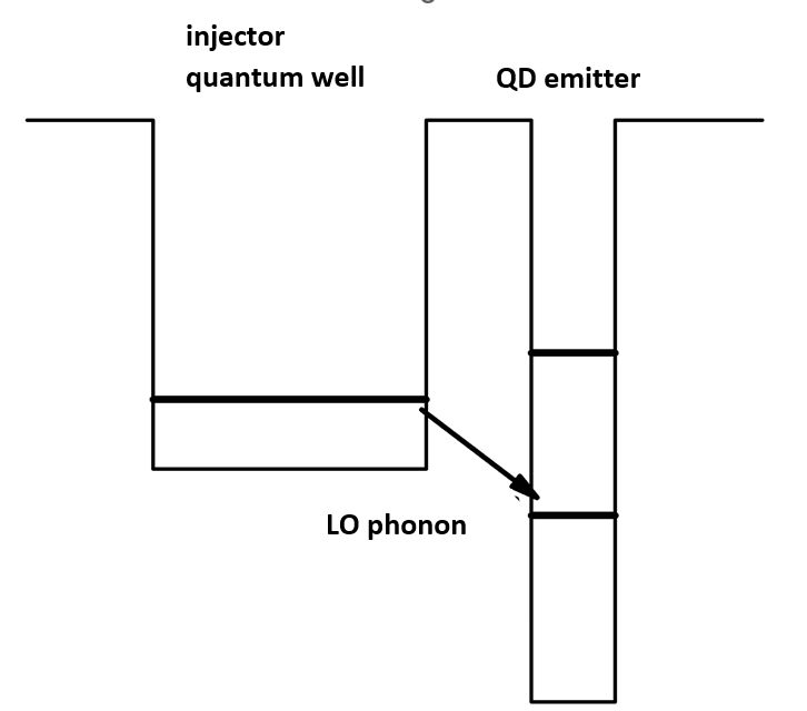
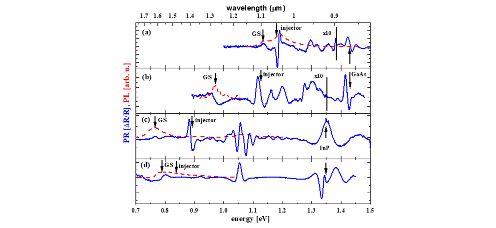
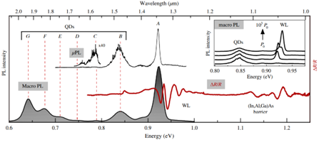
A potential solution for both issues is the application of hybrid structures, called tunnel injection structures. Laser active material is constituted by a quantum well, serving as a carrier reservoir and a layer of quantum dots (emitter), quantum mechanically coupled through a thin tunnelling barrier. A fundamental challenge is to design a layer structure of the device (thicknesses and compositions), where the ground state of the whole coupled system, for both electrons and holes, is localized in the QDs, with emission at the desired wavelength (ultimately at the telecom windows), while consecutive states are confined in the well and separated in energy from the ground state by a longitudinal optical phonon energy (around 30‑40 meV in the group III-V semiconductors, i.e. materials of choice for near infrared emitters). In this way optically generated, or in final devices electrically injected, carriers can be efficiently collected by a quantum well, which is characterised by higher density of states than a QD layer, thus increasing a carrier capture rate. Also, the thermalization within a well, due to a quasi-continuous ladder of confined states, is faster than in QDs. Next, the collected carriers tunnel from the lowest states in the well, through a thin barrier, preferably with the assist of optical phonons to ensure efficiency and directionality of the process, to the QD layer, where they recombine radiatively. A sketch of a conduction band and confined states for an ideal tunnel injection structure is shown above. A figure below shows photoreflectance and photoluminescence spectra obtained for tunnel injection structures realized in different material systems.
InAs quantum dots integrated with silicon
The need for materials enabling ever faster exchange and processing of data constitutes a major challenge facing material science. Although the majority of long distance communication is currently already carried over optical channels, a next technological step – replacement of electric links between individual computers or computer components with optical interconnects, or even a complete substitution of electronic devices with photonic counterparts – is required to sustain the growing needs of information society. Photonic integrated circuits (PIC) are already available, however, current solutions are generally neither cost-effective nor suitable for mass production. The most promising approach is to exploit technology compatible with the silicon-based complementary metal–oxide–semiconductor (CMOS) manufacturing platform. Although many passive elements are already realized, the indirect bandgap of silicon limits its use as material for light emitter. Therefore, it is necessary to include other semiconducting material in the device, such as InAs/GaAs or InAs/InP quantum dots.
There are many approaches to the integration of III-V direct bandgap semiconductors into silicon. The projects concerns mostly two of them, developed in the University of Kassel. One interesting way of direct growth of InAs quantum dots on Si is to utilize multi-step silicon overgrowth and annealing process performed by molecular beam epitaxy (MBE), resulting in nearly completely relaxed InAs quantum dots (more resembling nanocrystals at this stage) being embedded in a defect-free silicon matrix. The structural investigations show that the strain relaxation is mainly localized at the III-V silicon interface by closed dislocation loops surrounding the InAs nanocrystal, which can be further removed by using core-shell approach.
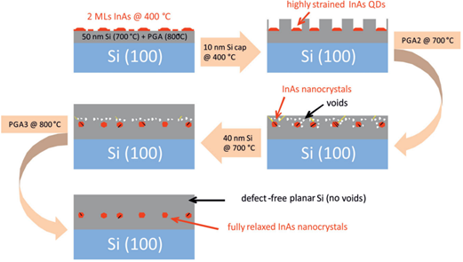
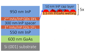
For longer wavelength emission (e.g., at 1550 nm) there are utilized InAs/InP quantum dots. To create optimal conditions for growth of this kind of dots on (001) silicon substrate (minimize unwanted defects within the InP crystal), multiple InAs/InP quantum dots are used as dislocation filters. Directly on (001) silicon, GaAs intermediate buffer is grown to accommodate the lattice mismatch, next there is deposited InP buffer layer, followed by few layers of InAs/InP quantum dots and finally capped by InP, providing high quality substrate for further growth of, e.g., optically active InAs/InP quantum dots.
The research objective is to investigate structural, electronic and optical properties of novel type of optically active materials based on III-V quantum dots, grown on silicon substrates or embedded in silicon matrices, hence compatible with CMOS silicon platform, in the context of developing active elements for future photonic integrated circuits. The studies will concern ensembles of QDs, to investigate their potential for laser and detector applications, but also properties of single QDs will be explored due to their relevance in more sophisticated applications, such as quantum communication or quantum computing schemes utilizing PICs.
Tuneable VCSEL arrays for water vapour detection
Vertical cavity surface emitting lasers (VCSELs) are used in many applications, including telecommunication or gesture-recognition technology and proximity sensing crucial for autonomous vehicles, robots and drones. A clear advantage of VCSELs with respect to conventional edge emitting lasers stems from their low power consumption, excellent beam quality, single mode operation and lower cost. Quantum dot based VCSEL emission spans the range from 750 to 1100 nm, which corresponds to the absorption lines of water vapour. Detection of water is required in numerous applications related to the petrochemical industry, climate monitoring, combustion control, engine optimization in automotive industry etc. This project aims at the development and implementation of VCSEL arrays meeting the requirements for laser sources used in water vapour detection. The novelty of the chosen approach is based on utilization of a monolithic high contrast grating (MHCG) as a top mirror, being a one-dimensional arrangement of equally spaced semiconductor stripes, implemented in the place of a bulk distributed Bragg reflector (DBR). MHCG enables post-growth resonant wavelength setting of VCSELs by tuning the reflection phase through variation of a period and width of the MHCG stripes. The investigated design will be also a proof of concept for integrated arrays of VCSELs each with different emission wavelength fabricated in a single process for different material systems, aimed at other applications.
QDs for telecom non-classical light sources
Plug&play single photon sources
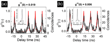
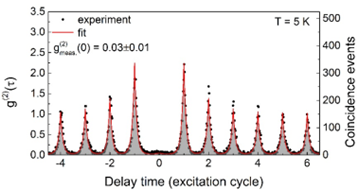
Single-photon sources are important resource for quantum technologies, in particular quantum communication and cryptography. An ideal source of single photons should emit exactly one photon following each excitation pulse and all emitted photons should be identical – indistinguishable from each other. Preferable are high excitation rates resulting in high emission rates and it should be possible to collect all emitted photons. For practical purposes such device should operate at room temperature in a plug&play fashion and the energy of emitted photons should be in the range of telecommunication windows – the spectral range for which attenuation in the optical fibres is minimal (O-band – wavelengths around 1310 nm suitable for local quantum networks and C-band – around 1550 nm – offering minimal signal loss). The latter allows maximizing the transmission distance and therefore length of quantum link for which quantum repeater is not required. Different physical systems are considered to best fulfil abovementioned requirements. We are focusing on investigating epitaxial quantum dots (QDs) in photonics structures in different III-V semiconductor material systems (see below) for this purpose.
A demonstrator of such a device – a single-photon source operating at the telecom O-band has been realized and further used to implement quantum key distribution protocols by Quantum Communication Systems group led by Tobias Heindel at Technical University of Berlin.

In this particular case, an emitter was a single InAs/GaAs QD incorporated deterministically into a cylindrical mesa by in-situ cathodoluminescence lithography technique developed in Optoelectronics and Quantum Devices group led by Stephan Reitzenstein at Technical University of Berlin. Emission in the O-band was achieved owing to an InGaAs strain reducing layer on top of the active material. The exact mesa geometry was optimized numerically to maximize the extraction efficiency by collaborators from Zuse Institute in Berlin, using JCM Suite software implemented by them. A specialty high numerical aperture single mode fiber, designed by Fiber Optics group from Wroclaw University of Science and Technology, was fabricated at Maria Curie-Skłodowska University. An interference-based technique for positioning and technology for creating a rigid link between the fiber and a QD in a photonic structure has been developed at Fiber Optics Group. For the final demonstrator, a specialized fiber components (coupler, filters) and low loss splice to a standard telecom fiber has been prepared by Fibrain company from Rzeszów. This joint effort was financially supported by NCBR and IBB within a Poland-Berlin/Brandenburg programme in the field of photonics.
InAs/GaAs QDs
One of the approaches to reach telecommunication spectral range is to take advantage of mature GaAs semiconductor technology and engineer strain in the structure to allow growth of larger, less strained QDs. This is needed because of the relatively large lattice constants mismatch (7%) between InAs and GaAs alloys.
The possible strain engineering approaches are:
1) To cap QDs with low In content strain reducing InGaAs layer
These QDs are provided by the group of prof. Reitzenstein from Technical University of Berlin (MOCVD) and allowed building the demonstrator of plug&play single-photon source operating at the telecom O-band.
2) To provide virtual substrate for growth of InAs QDs using metamorphic buffer layer (MBL)
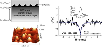
These nanostructures are grown by MBE at University of Würzburg in group of prof. Sven Höfling and allowed redshifting the emission to the telecom C‑band.
InAs/(InGaAlAs)/InP QDs
The other material system developed for emission at telecommunication wavelengths is based on InP substrates. These QDs emit naturally at longer wavelengths in comparison to GaAs‑substrate‑ structures, because of lower strain resulting from lower lattice constants mismatch of 2%. However, it was challenging to isolate a single quantum emitter and involved a lot of engineering and growth optimization to reach low spatial density. This has been achieved in the group of prof. Reithmaier and dr. Benyoucef at the University of Kassel, using MBE growth technique.
Additionally, the first growth attempts resulted in strongly elongated structures, so called quantum dashes (QDash), which featured relatively dense ladder of quantized states due to large size, with more than 100 nm length in one of the in‑plane directions. These types of structures grown by MBE at University of Würzburg in group of prof. Höfling allowed demonstrating single‑photon emission in InAs/InP material system up to 80 K and determining properties of excitonic complexes.
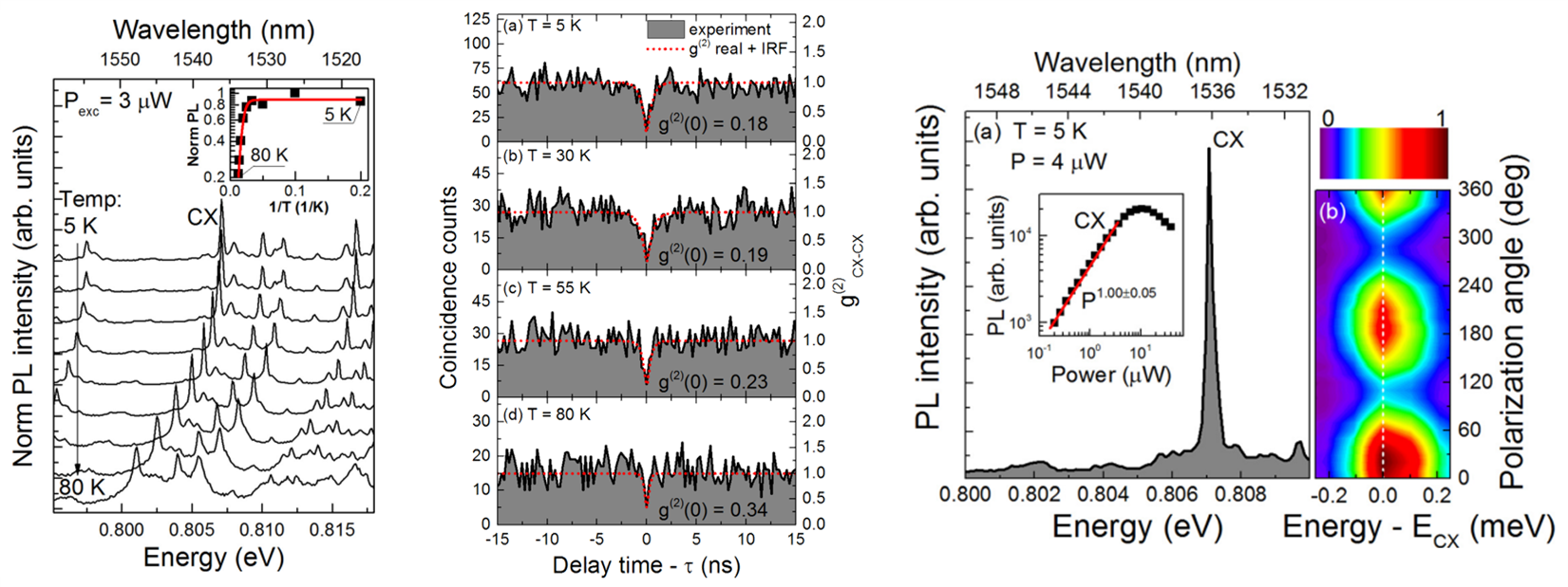
Another challenge that has been addressed is the in‑plane symmetry of the nanostructures. Successful attempts to modify the MBE growth, by adding ripeningૹstep to the growth protocol, in the group of prof. Reithmaier and dr. Benyoucef at the University of Kassel, resulted in symmetric InAs QDs, embedded directly in the InP matrix and emitting at the telecom C‑band. This allows not only reaching high‑purity single‑photon emission, but also generation of polarization‑entangled photons from biexciton‑exciton cascade.
